MIC39150/39151/39152
1.5A, Low-Voltage Low-Dropout
Regulator
General Description
Features
The MIC39150, MIC39151, and MIC39152 are 1.5A LDO
voltage regulators that provide a low voltage, high current
output with a minimum of external components. Utilizing
Micrel’s proprietary Super βeta PNP® pass element, the
MIC39150/1/2 offers extremely low dropout (typically
375mV at 1.5A) and low ground current (typically 17mA at
1.5A).
• 1.5A minimum guaranteed output current
• 500mV maximum dropout voltage over temperature
– Ideal for 3.0V to 2.5V conversion
– Ideal for 2.5 to 1.8V or 1.65V conversion
• 1% initial accuracy
• Low ground current
• Current limiting and Thermal shutdown
• Reversed-battery and reversed lead insertion protection
• Reversed-leakage protection
• Fast transient response
• TTL/CMOS compatible enable pin (MIC39151/2 only)
• Error flag output (MIC39151 only)
• Adjustable output (MIC39152 only)
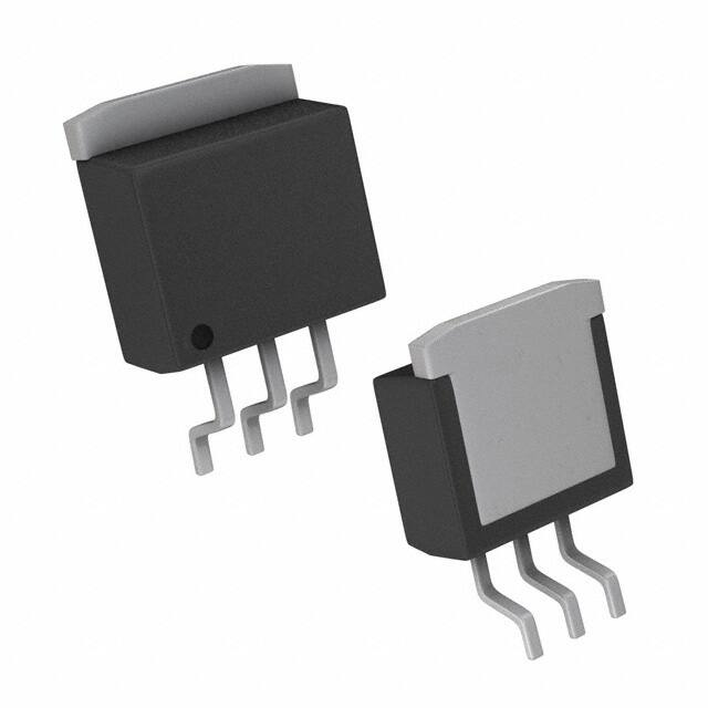
• Power D-Pak package (TO-252) Adjustable only
• Power D2Pak package (TO-263)
The MIC39150/1/2 are ideal for PC add-in cards that need
to convert from 3.3V to 2.5V or 2.5V to 1.8V with a
guaranteed maximum dropout voltage of 500mV over all
operating conditions. The MIC39150/1/2 exhibit fast
transient response for heavy switching applications and
requires only 10µF of output capacitance to maintain
stability and achieve fast transient response.
The MIC39150/1/2 is fully protected with current limiting,
thermal shutdown, reversed-battery protection/lead
insertion, and reverse-leakage protection. The MIC39151
offers a TTL-logic compatible enable pin and an error flag
that indicates undervoltage and overcurrent conditions.
Offered in fixed voltages of 2.5V, 1.8V and 1.65V, the
MIC39150/1 comes in the TO-220 and TO-263 (D2Pak)
packages. The MIC39152 adjustable option allows
programming the output voltage anywhere between 1.24V
and 15.5V and comes in 5-Pin, TO-263 (D2Pak) and
TO-252 (D-Pak) packages.
For applications requiring input voltage greater than 16V or
automotive load dump protection, see the MIC29150/1/2/3
family.
Applications
•
•
•
•
•
•
Low-voltage digital ICs
LDO linear regulator for PC add-in cards
High-efficiency linear power supplies
SMPS post regulator
Low-voltage microcontrollers
StrongARM™ processor supply
Typical Application**
MIC39150
MIC39151
MIC39152 Adjustable Output Application
(*See Minimum Load Current Section)
**See Thermal Design Section
Super ßeta PNP is a registered trademark of Micrel, Inc.
StrongARM is a trademark of Advanced RSIC Machines, Ltd.
Micrel Inc. • 2180 Fortune Drive • San Jose, CA 95131 • USA • tel +1 (408) 944-0800 • fax + 1 (408) 474-1000 • http://www.micrel.com
October 2009
M9999-102309-A
�Micrel, Inc.
MIC39150/39151/39152
Ordering Information
Part Number
Standard
Junction
Temp. Range
Voltage
RoHS Compliant*
Package
MIC39150-1.65BT
MIC39150-1.65WT
1.65V
–40° to +125°C
3-Pin TO-220
MIC39150-1.65BU
MIC39150-1.65WU
1.65V
–40° to +125°C
3-Pin TO-263
MIC39150-1.8BT
MIC39150-1.8WT
1.8V
–40° to +125°C
3-Pin TO-220
MIC39150-1.8BU
MIC39150-1.8WU
1.8V
–40° to +125°C
3-Pin TO-263
MIC39150-2.5BT
MIC39150-2.5WT
2.5V
–40° to +125°C
3-Pin TO-220
MIC39150-2.5BU
MIC39150-2.5WU
2.5V
–40° to +125°C
3-Pin TO-263
MIC39151-1.65BT
MIC39151-1.65WT
1.65V
–40° to +125°C
5-Pin TO-220
MIC39151-1.65BU
MIC39151-1.65WU
1.65V
–40° to +125°C
5-Pin TO-263
MIC39151-1.8BT
MIC39151-1.8WT
1.8V
–40° to +125°C
5-Pin TO-220
MIC39151-1.8BU
MIC39151-1.8WU
1.8V
–40° to +125°C
5-Pin TO-263
MIC39151-2.5BT
MIC39151-2.5WT
2.5V
–40° to +125°C
5-Pin TO-220
MIC39151-2.5BU
MIC39151-2.5WU
2.5V
–40° to +125°C
5-Pin TO-263
—
MIC39152WU
Adjustable
–40° to +125°C
5-Pin TO-263
—
MIC39152WD
Adjustable
–40° to +125°C
5-Pin TO-252
Note:
* RoHS compliant with ‘high-melting solder’ exemption.
October 2009
2
M9999-102309-A
�Micrel, Inc.
MIC39150/39151/39152
Pin Configuration
3
OUT
3
OUT
2
GND
2
GND
1
IN
1
IN
MIC39150-x.xBT/WT
TO-220-3 (T)
MIC39150-x.xBU/WU
TO-263-3 (U)
5
4
3
2
1
FLG
OUT
GND
IN
EN
MIC39151-x.xBT/WT
TO-220-5 (T)
MIC39151-x.xBU/WU
TO-263-5 (D2Pak) (U)
MIC39152WU
2
TO-263-5 (D Pak) (U))
MIC39152WD
TO-252-5 (D-Pak) (D)
Pin Description
Pin Number
MIC39150
Pin Number
Pin Number
MIC39151
MIC39152
—
1
1
Pin Name
Pin Description
Enable (Input): TTL/CMOS compatible input. Logic high =
enable; logic low or open = shutdown.
EN
1
2
2
IN
2, TAB
3, TAB
3, TAB
GND
Ground: Ground pin and TAB are internally connected.
3
4
4
OUT
Regulator Output.
—
5
—
FLG
Error Flag (Output): Open-collector output. Active low
indicates an output fault condition.
—
—
5
ADJ
Adjustable Regulator Feedback Input: Connect to the
resistor voltage divider that is placed from OUT to GND in
order to set the output voltage.
October 2009
Unregulated Input: +16V maximum supply.
3
M9999-102309-A
�Micrel, Inc.
MIC39150/39151/39152
Absolute Maximum Ratings(1)
Operating Ratings(2)
Supply Voltage (VIN) ....................................... –20V to +20V
Enable Voltage (VEN)....................................................+20V
Storage Temperature (Ts) .........................–60°C to +150°C
Lead Temperature (soldering, 5 sec.)........................ 260°C
ESD Rating................................................................ Note 3
Supply Voltage (VIN).................................... +2.25V to +16V
Enable Voltage (VEN)....................................................+16V
Maximum Power Dissipation (PD(max)) ....................... Note 4
Junction Temperature (TJ) ........................ –40°C to +125°C
Package Thermal Resistance
TO-263 (θJC) ........................................................2°C/W
TO-220 (θJC) ........................................................2°C/W
TO-252 (θJC) ........................................................3°C/W
TO-252 (θJA) ......................................................56°C/W
Electrical Characteristics(5)
VIN = VEN = VOUT + 1V; IOUT = 10mA; TJ = 25°C, bold values indicate –40°C< TJ < +125°C, unless noted.
Symbol
Parameter
Condition
VOUT
Output Voltage
10mA
10mA ≤ IOUT ≤ 1.5A, VOUT + 1V ≤ VIN ≤ 8V
Line Regulation
IOUT = 10mA, VOUT + 1V ≤ VIN ≤ 16V
Load Regulation
VIN = VOUT + 1V, 10mA ≤ IOUT ≤ 1.5A
∆VOUT/∆T
Output Voltage Temp.
Coefficient, Note 6
VDO
Dropout Voltage, Note 7
IGND
Ground Current, Note 8
Min
Typ
Max
Units
1
2
%
%
0.06
0.5
%
0.2
1
%
20
100
ppm/°C
80
200
mV
–1
–2
IOUT = 100mA, ∆VOUT = –1%
IOUT = 750mA, ∆VOUT = –1%
260
IOUT = 1.5A, ∆VOUT = –1%
375
500
mV
mV
IOUT = 750mA, VIN = VOUT + 1V
4
20
mA
IOUT = 1.5A, VIN = VOUT + 1V
17
mA
IGND(do)
Dropout Ground Pin Current
VIN ≤ VOUT(nominal) – 0.5V, IOUT = 10mA
1.1
mA
IOUT(lim)
Current Limit
VOUT = 0V, VIN = VOUT + 1V
2.8
A
IOUT(min)
Minimum Load Current
tSTART
Start-up Time
VEN = VIN, IOUT = 10mA, COUT = 47µF
7
10
mA
35
150
µs
0.8
V
Enable Input (MIC39151)
VEN
Enable Input Voltage
logic low (off)
logic high (on)
IIN
Enable Input Current
V
2.25
VEN = 2.25V
1
30
75
µA
µA
2
4
µA
µA
10
20
µA
15
VEN = 0.8V
IOUT(shdn)
Shutdown Output Voltage
Note 9
Flag Output (MIC39151)
IFLG(leak)
Output Leakage Current
VOH = 16V
0.01
1
2
µA
µA
VFLG(do)
Output Low Voltage
VIN = 2.250V, IOL = 250µA, Note 10
180
300
400
mV
mV
VFLG
Low Threshold
% of VOUT
High Threshold
% of VOUT
93
99.2
Hysteresis
October 2009
%
1
4
%
%
M9999-102309-A
�Micrel, Inc.
Symbol
MIC39150/39151/39152
Parameter
Condition
Min
Typ
Max
Units
1.228
1.240
1.252
V
1.265
V
Reference (Adjust Pin) – MIC39152 Only
VADJ
Reference Voltage
1.215
VTC
Reference Voltage Temperature
ppm/°C
20
Note 11
Coefficient
IADJ
Adjust Pin Bias Current
40
80
nA
120
nA
Notes:
1. Exceeding the absolute maximum rating may damage the device.
2. The device is not guaranteed to function outside its operating rating.
3. Devices are ESD sensitive. Handling precautions recommended.
4. PD(max) = (TJ(max) – TA) ÷ θJA, where θJA depends upon the printed circuit layout. See “Applications Information.”
5. Specification for packaged product only.
6. Output voltage temperature coefficient is ∆VOUT(worst case) ÷ (TJ(max) – TJ(min)) where T J(max) is +125°C and TJ(min) is –40°C.
7. VDO = VIN – VOUT when VOUT decreases to 98% of its nominal output voltage with VIN = VOUT + 1V. For output voltages below 2.25V, dropout voltage is
the input-to-output voltage differential with the minimum input voltage being 2.25V. Minimum input operating voltage is 2.25V.
8. IGND is the quiescent current. IIN = IGND + IOUT.
9. VEN ≤ 0.8V, VIN ≤ 8V, and VOUT = 0V.
10. For a 2.5V device, VIN = 2.250V (device is in dropout).
11. Thermal regulation is defined as the change in output voltage at a time t after a change in power dissipation is applied, excluding load or line
regulation effects. Specifications are for a 200mA load pulse at VIN = 8V for t = 10ms.
October 2009
5
M9999-102309-A
�Micrel, Inc.
MIC39150/39151/39152
Typical Characteristics
Power Supply
Rejection Ratio
60
VIN = 3.3V
VOUT = 2.5V
50
40
30
20
ILOAD = 1.5A
10 COUT = 10µF
CIN = 0
0
1E+1
1k 1E+4
10k 1E+5
1M
10 1E+2
100 1E+3
100k 1E+6
FREQUENCY (Hz)
2.6
500
400
2.8
2.4
VOUT = 1.8V
300
ILOAD = 100mA
15
1.4
ILOAD = 750mA
1.2
5
VOUT = 2.5V
0
0
INPUT VOLTAGE (V)
65
60
55
50
45
40
35
30
25
20
15
10
5
0
Ground Current
vs. Supply Voltage
ILOAD = 1000mA
ILOAD = 750mA
Ground Current
vs. Temperature
0.34
0
2
4
6
8
10 12
SUPPLY VOLTAGE (V)
Ground Current
vs. Temperature
VOUT = 2.5V
15
VOUT = 1.8V
0.33
0.32 V
= 2.5V
OUT
0.31
20
ILOAD = 10mA
0.30
-40 -20 0 20 40 60 80 100 120
TEMPERATURE °C)
(
3.5
3.0
2.5
Short Circuit vs.
Temperature
typical 2.5V device
typical 1.8V device
2.0
VOUT = 1.8V
1.5
10
5
0.36
250 500 750 100012501500
OUTPUT CURRENT (mA)
0.35
ILOAD = 1500mA
25
ILOAD = 1.5A
1.0
0.5
0
-40 -20 0 20 40 60 80 100 120
TEMPERATURE °C)
(
October 2009
VOUT = 1.8V
10
ILOAD = 1.5A
1.6
0
-40 -20 0 20 40 60 80 100 120
TEMPERATURE °C)
(
25
2.0
1.8
ILOAD = 1.5A
Ground Current
vs. Output Current
20
2.2
VOUT = 2.5V
200
100
Dropout Characteristics
1.4
1.6
1.8
2
2.2
2.4
2.6
2.8
3
3.2
3.4
3.6
600
Dropout Voltage
vs. Temperature
6
0
-40 -20 0 20 40 60 80 100 120
TEMPERATURE °C)
(
M9999-102309-A
�Micrel, Inc.
6
5
4
MIC39150/39151/39152
Error Flag
Pull-Up Resistor
VIN = 5V
FLAG HIGH
(OK)
3
2
FLAG LOW
(FAULT)
1
0
0.01 0.1
1
10 100 100010000
RESISTANCE (k )
October 2009
7
M9999-102309-A
�Micrel, Inc.
MIC39150/39151/39152
Functional Characteristics
October 2009
8
M9999-102309-A
�Micrel, Inc.
MIC39150/39151/39152
Functional Diagram
IN
OUT
O.V.
ILIMIT
FLAG*
1.180V
Ref.
18V
1.240V
EN*
Thermal
Shutdown
GND
* MIC39151 only
October 2009
9
M9999-102309-A
�Micrel, Inc.
MIC39150/39151/39152
distribute the heat between this resistor and the
regulator. The low dropout properties of Micrel Super
βeta PNP® regulators allow significant reductions in
regulator power dissipation and the associated heat sink
without compromising performance. When this technique
is employed, a capacitor of at least 1µF is needed
directly between the input and regulator ground.
Refer to Application Note 9 for further details and
examples on thermal design and heat sink specification.
Application Information
The MIC39150/1/2 are high-performance, low-dropout
voltage regulators suitable for moderate to high-current
voltage regulator applications. Its 500mV dropout
voltage at full load and overtemperature makes it
especially valuable in battery-powered systems and as
high-efficiency noise filters in post-regulator applications.
Unlike older NPN-pass transistor designs, where the
minimum dropout voltage is limited by the base-toemitter voltage drop and collector-to-emitter saturation
voltage, dropout performance of the PNP output of these
devices is limited only by the low VCE saturation voltage.
With no heat sink in the application, calculate the
junction temperature to determine the maximum power
dissipation that will be allowed before exceeding the
maximum junction temperature of the MIC39152. The
maximum power allowed can be calculated using the
thermal resistance (θJA) of the TO-252 (D-Pak) adhering
to the following criteria for the PCB design: 2 oz. copper
and 100mm2 copper area for the MIC39152.
For example, given an expected maximum ambient
temperature (TA) of 75°C with VIN = 2.25V, VOUT = 1.75V,
and IOUT = 1.5A, first calculate the expected PD using
Equation (1);
PD = (2.25V – 1.75V)1.5A + (2.25V)(0.017A) = 0.788W
Next, calcualte the junction temperature for the expected
power dissipation.
A trade-off for the low dropout voltage is a varying base
drive requirement. Micrel’s Super βeta PNP® process
reduces this drive requirement to only 2% to 5% of the
load current. The MIC39150/1/2 regulators are fully
protected from damage due to fault conditions. Current
limiting is provided. This limiting is linear; output current
during overload conditions is constant. Thermal
shutdown disables the device when the die temperature
exceeds the maximum safe operating temperature.
Transient protection allows device (and load) survival
even when the input voltage spikes above and below
nominal. The output structure of these regulators allows
voltages in excess of the desired output voltage to be
applied without reverse current flow.
TJ = (θJA × PD) + TA = (56°C/W × 0.788W) + 75°C
Thermal Design
Linear regulators are simple to use. The most
complicated design parameters to consider are thermal
characteristics. Thermal design requires the following
application-specific parameters:
= 119.14°C
Now determine the maximum power dissipation allowed
that would not exceed the IC’s maximum junction
temperature (125°C) without the use of a heat sink by
PD(MAX) = (TJ(MAX) – TA)/θJA = (125°C – 75°C)/(56°C/W)
= 0.893W
• Maximum ambient temperature (TA)
• Output Current (IOUT)
• Output Voltage (VOUT)
• Input Voltage (VIN)
• Ground Current (IGND)
First, calculate the power dissipation of the regulator
from these numbers and the device parameters from this
datasheet.
VIN
CIN
MIC39150-x.x
IN
OUT
GND
VOU T
COU T
PD = (VIN − VOUT ) IOUT + VIN IGND
Figure 1. Capacitor Requirements
where the ground current is approximated by using
numbers from the “Electrical Characteristics” or “Typical
Characteristics.” Then the heat sink thermal resistance is
determined with this formula:
θ SA =
TJ(max) − TA
PD
Output Capacitor
The MIC39150/1/2 requires an output capacitor to
maintain stability and improve transient response. See
Figure 1. Proper capacitor selection is important to
ensure proper operation. TheMIC39150/1/2 output
capacitor selection is dependent upon the ESR
(equivalent series resistance) of the output capacitor to
maintain stability. When the output capacitor is 10µF or
greater, the output capacitor should have an ESR less
than 2Ω. This will improve transient response as well as
− (θ JC + θ CS )
Where TJ(max) ≤ 125°C and θCS is between 0° and 2°C/W.
The heat sink may be significantly reduced in
applications where the minimum input voltage is known
and is large compared with the dropout voltage. Use a
series input resistor to drop excessive voltage and
October 2009
10
M9999-102309-A
�Micrel, Inc.
MIC39150/39151/39152
promote stability. Ultralow ESR capacitors (